Description

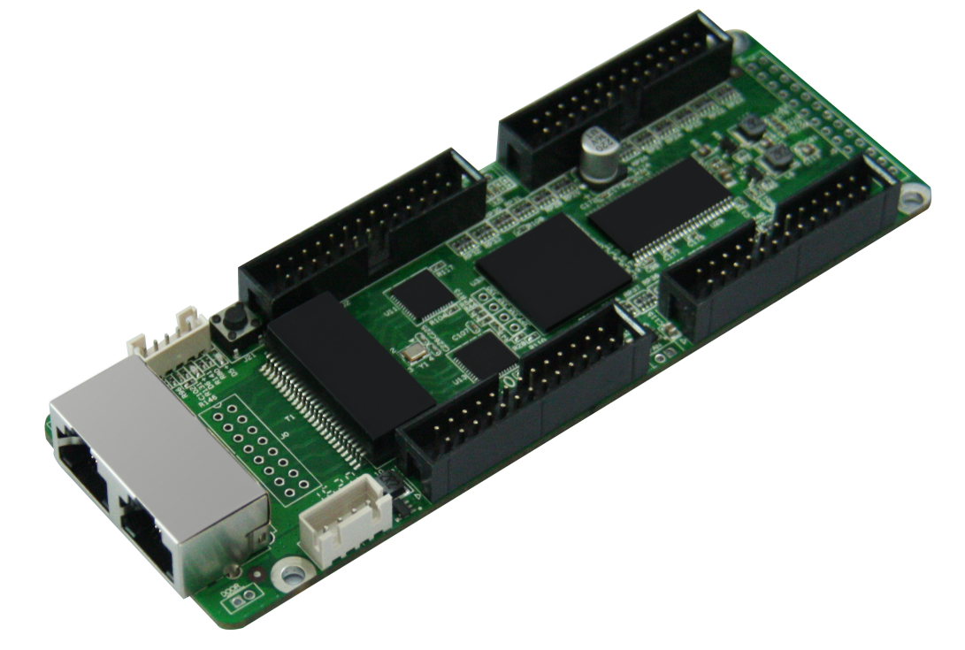
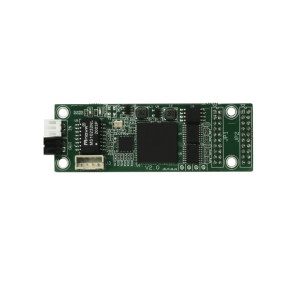
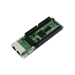
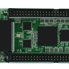
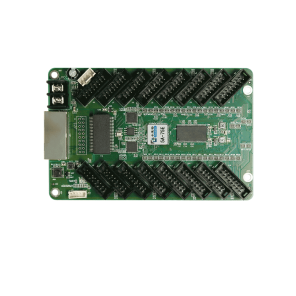
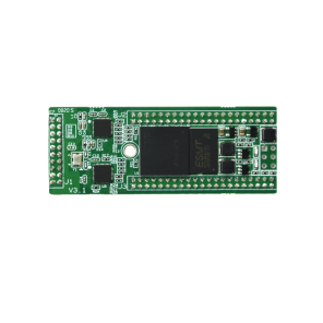
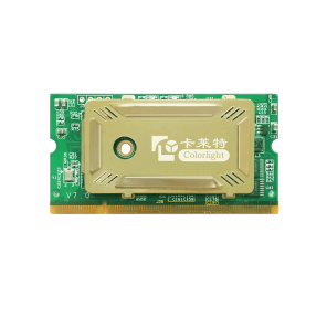
Colorlight i5A-907 Receiving Card
Overview
Colorlight i5A-907 Receiving Card is usually used for the LED video walls, small spacing LED display, LED car screen due to the smaller size.
Features
- Tiny size, special designed for the compact structure designs, like color screen and casting aluminum cabinet.
- Power supply from pin board without the need of external power supply, enhance hardware stability.
- New processing core, perfect in display effect.
- High refresh rate, high gray scale and high brightness with conventional chips.
- Perfect performance under lower grayscale status.
- Better detail processing: Partial dark at row, reddish at low gray, shadow problems can be solved.
- Support the effective display at first grayscale value.
- Support 14 bits high-precision point-by-point calibration in the Brightness and chromaticity.
- Support conventional chips, PWM chips and lighting chips, etc.
- Support any scan mode from static to 1/32 scan.
- Support any pumping point and data arbitrary offset, and realize various freeform display, spherical display, diamond display, creative display, etc.
- Support 16 groups RGBR’ signal output and 24 groups RGB in maximum.
- Large load capacity.
- Advanced design, high quality components, rigorous aging test, zero malfunction of final products.
- Wide working voltage range with DC 3.3 -6V.
- Support dual receiving card backup, loop backup, and dual-machine backup, etc.
- Compatible with S series Sender, Z series Sender and C series Sender, etc.
Specifications
Hardware
2. Signal output definitions
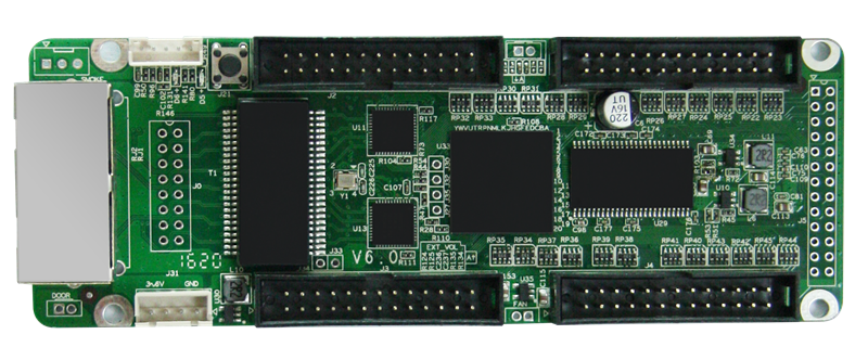
i5A-907 has five 26P data output interface, and J5 and J1 output the same data. J5 is a horizontal interface, for the special structure using.
i5A-907 supports different work modes, and 26P output interface definitions are different in each work mode, which shown as follows:
2.1 Standard Mode (Default Mode)
2.2 20 Groups Mode
| JI/J5 | J2 | J3 | J4 | ||||||||||||
| 1 | A | B | 2 | 1 | A | B | 2 | 1 | A | B | 2 | 1 | A | B | 2 |
| 3 | OE | LAT | 4 | 3 | OE | LAT | 4 | 3 | OE | LAT | 4 | 3 | OE | LAT | 4 |
| 5 | CLK | VCC | 6 | 5 | CLK | VCC | 6 | 5 | CLK | VCC | 6 | 5 | CLK | VCC | 6 |
| 7 | C | D | 8 | 7 | C | D | 8 | 7 | C | D | 8 | 7 | C | D | 8 |
| 9 | E | R1 | 10 | 9 | E | R6 | 10 | 9 | E | R11 | 10 | 9 | E | R16 | 10 |
| 11 | G1 | B1 | 12 | 11 | G6 | B6 | 12 | 11 | G11 | B11 | 12 | 11 | G16 | B16 | 12 |
| 13 | GND | R2 | 14 | 13 | GND | R7 | 14 | 13 | GND | R12 | 14 | 13 | GND | R17 | 14 |
| 15 | G2 | B2 | 16 | 15 | G7 | B7 | 16 | 15 | G12 | B12 | 16 | 15 | G17 | B17 | 16 |
| 17 | R3 | G3 | 18 | 17 | R8 | G8 | 18 | 17 | R13 | G13 | 18 | 17 | R18 | G18 | 18 |
| 19 | B3 | GND | 20 | 19 | B8 | GND | 20 | 19 | B13 | GND | 20 | 19 | B18 | GND | 20 |
| 21 | R4 | G4 | 22 | 21 | R9 | G9 | 22 | 21 | R14 | G14 | 22 | 21 | R19 | G19 | 22 |
| 23 | B4 | R5 | 24 | 23 | B9 | R10 | 24 | 23 | B14 | R15 | 24 | 23 | B19 | R20 | 24 |
| 25 | G5 | B5 | 26 | 25 | G10 | B10 | 26 | 25 | G15 | B15 | 26 | 25 | G20 | B20 | 26 |
2.3 24 Groups Mode
Include A and B scan signal;For 1/4~1/32, there need a serial decoding circuit as shown below.
| JI/J5 | J2 | J3 | J4 | ||||||||||||
| 1 | A | B | 2 | 1 | A | B | 2 | 1 | A | B | 2 | 1 | A | B | 2 |
| 3 | OE | LAT | 4 | 3 | OE | LAT | 4 | 3 | OE | LAT | 4 | 3 | OE | LAT | 4 |
| 5 | CLK | VCC | 6 | 5 | CLK | VCC | 6 | 5 | CLK | VCC | 6 | 5 | CLK | VCC | 6 |
| 7 | R1 | G1 | 8 | 7 | R7 | G7 | 8 | 7 | R13 | G13 | 8 | 7 | R19 | G19 | 8 |
| 9 | B1 | R2 | 10 | 9 | B7 | R8 | 10 | 9 | B13 | R14 | 10 | 9 | B19 | R20 | 10 |
| 11 | G2 | B2 | 12 | 11 | G8 | B8 | 12 | 11 | G14 | B14 | 12 | 11 | G20 | B20 | 12 |
| 13 | GND | R3 | 14 | 13 | GND | R9 | 14 | 13 | GND | R15 | 14 | 13 | GND | R21 | 14 |
| 15 | G3 | B3 | 16 | 15 | G9 | B9 | 16 | 15 | G15 | B15 | 16 | 15 | G21 | B21 | 16 |
| 17 | R4 | G4 | 18 | 17 | R10 | G10 | 18 | 17 | R16 | G16 | 18 | 17 | R22 | G22 | 18 |
| 19 | B4 | GND | 20 | 19 | B10 | GND | 20 | 19 | B16 | GND | 20 | 19 | B22 | GND | 20 |
| 21 | R5 | G5 | 22 | 21 | R11 | G11 | 22 | 21 | R17 | G17 | 22 | 21 | R23 | G23 | 22 |
| 23 | B5 | R6 | 24 | 23 | B11 | R12 | 24 | 23 | B17 | R18 | 24 | 23 | B23 | R24 | 24 |
| 25 | G6 | B6 | 26 | 25 | G12 | B12 | 26 | 25 | G18 | B18 | 26 | 25 | G24 | B24 | 26 |
2.4 16 Groups Serial Mode
Only J1 and J5 works, output the same data, choose between, detailed definition as belows:
| JI/J5 | |||
| 1 | A | B | 2 |
| 3 | OE | LAT | 4 |
| 5 | CLK | VCC | 6 |
| 7 | C | D | 8 |
| 9 | R1 | R2 | 10 |
| 11 | R3 | R4 | 12 |
| 13 | GND | R5 | 14 |
| 15 | R6 | R7 | 16 |
| 17 | R8 | R9 | 18 |
| 19 | R10 | GND | 20 |
| 21 | R11 | R12 | 22 |
| 23 | R13 | R14 | 24 |
| 25 | R15 | R16 | 26 |
3. Serial decoding circuit
4. External interface definition
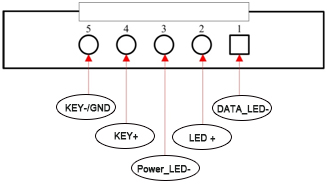
5. Power interface pin definition
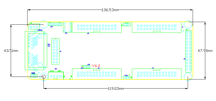
6. Figure for receiving card size and hole position
